


Glossar
A
AD-Converter: It converts an analogue signal into digital values. In digital cameras the AD-converter is an electronic device in which the voltage signal for each pixel of the sensor is transformed into discrete numbers. The values for every pixel form the digital representation of the detected image. Scientific cameras typically use precise AD converters having a resolution of 16bit or 65536 gray scales.
Advanced inverted mode operation (AIMO): AIMO sensors have a modified gate structure which reduces the dark current at the silicon-silicon dioxide interface. The full-well capacity is improved compared with the IMO sensors.
Anti-reflection coating: The surface of the sensor is coated with a layer of transparent dielectric material with a refractive index between that of sensor material and air in order to reduce the loss of light due to reflection. The coating is adapted to a certain wavelength range. Sensors with different coatings are available.
B
Back-illuminated: In order to improve the overall quantum efficiency, especially for blue and UV-light, back-illuminated sensor has been developed. The silicon wafer gets flipped during manufacturing and thinned by mechanical grinding and chemical etching. The incoming light is directed onto the backside of the sensor. Therefore the absorption and reflection loss, which occur on the front side due to the gate structure, are eliminated. Hence back-illuminated sensors have an enhanced quantum efficiency compared with front-illuminated sensors. Photons with wavelength in the blue and UV ranges have short absorption depth. The benefit of thinning the silicon is that the light can enter directly into the photosensitive region without passing through a thick layer of silicon. Furthermore, deep depletion back-illuminated sensors increase the light sensitivity in the near infrared and X-ray ranges up to 20keV for direct detection. Anti-reflection coatings and special surface passivation can improve the quantum efficiency in the visible, UV or EUV ranges.
Binning: Pixel binning is the summation of signal charge from adjacent pixels. Binning can be performed for pixels of the same column or of the same row. The advantages are less readout noise at the same frame rate and higher frame rate compared with the same readout frequency without binning. The disadvantage is the reduced spatial resolution of the detected image.
Blemish specifications: CCD sensors may contain different pixel defects after production. Traps are the defect pixels where charge is temporarily held. Black Spots are defect pixels when they have responsivity less than 90% of the local mean signal. White Spots are pixels when they have much higher dark current than neighbouring pixels. Black or White Column Defects are defects which contain a combination of Black or White Spots. Different blemish grades of sensors contain different numbers of Traps, Black/White Spots, and Black/White Column Defects. For detailed blemish specification of a certain sensor, please inquire us for more information.
Blooming: When the CCD is overexposed, the amount of generated electrons in the pixels exceed their full-well capacity. The overflow of generated excess electrons into adjacent pixels is called blooming.
Broadband coating: An anti-reflection coating optimized for a broad wavelength range in the visible spectrum.
Burst mode: In burst-mode the camera takes a number of image frames under predefined parameters like binning or crop mode at fixed delay or trigger events. The frames are streamed to the PC based on a single request. Burst mode allows precise and fast time-sequenced measurements.
C
CCD Sensor: A charged coupled device (CCD) is an image sensor in which the generated and accumulated charge is shifted pixel by pixel by applying an electric potential to insulated electrodes on the surface of the sensor. The charge is transferred to an output node on the chip. Due to their low noise and high sensitivity, CCDs are ideal for spectroscopy and optical imaging applications of low light signals and enable measurements with a high dynamic range.
Crop mode: Crop mode is a specialized readout mode for achieving fast frame rates. In this mode the user defines a number of lines above the readout register. The camera is directed to read out only defined lines. The smaller the defined array size, the faster the frame rate achievable. The crop mode is ideal for applications which demand fast temporal resolution. The rest of the sensor area must be shielded against incoming light.
D
Dark noise: Thermal excitation of charge carriers in the sensor due to defects in the silicon causes a dark current. The dark noise is the standard derivation of the dark current in the device. Dark noise can be reduced by cooling the sensor. The dark noise varies among different sensor architectures. In case of CCDs, non-inverted mode sensors (NIMO) have a higher dark noise in comparison with advanced inverted mode (AIMO) sensors.
Deep depletion : The quantum efficiency for near-infrared light and for direct detection of X-ray photons up to 20keV can be improved by a deeper depletion region which is realized through different doping of the sensor material. Photons in the abovementioned spectral region penetrate deeper into the silicon and are collected more efficiently by deep depletion sensors compared to conventional CCDs.
Depletion region: A space in the silicon in which an electrostatic field forces electrons to drift in the potential well. The width of the depletion region depends also on the doping of the silicon.
Dynamic range: The dynamic range is the ratio of the maximum to the minimum signal distinguishable from the noise. The maximum dynamic range of image sensors is the ratio of full well capacity to read noise.
E
Electro-mechanical shutter: Used to block the incoming light from the sensor during readout to prevent image smearing. It consists typically of an iris diaphragm which can be opened and closed by using an electromagnetic coil. This mechanism can be controlled by the camera, for example in such a way that the shutter is open during the exposure time and closed during readout.
Enhanced process: Surface passivation (enhanced process) of the backside of the sensor reduces light reflection and therefore improves the quantum efficiency especially in the UV and deep UV region.
Etaloning: NIR rays that enter a back-illuminated sensor are reflected at the interface between the silicon region and the gate at the back of the sensor due to a refraction index mismatch. Further reflections occur within the silicon making it act like an etalon. These reflections lead to a distorted output image seen as fringes of constructive and destructive interference. This can be reduced through fringe suppression techniques.
F
Full-frame CCD image sensor: In a full-frame image sensor, the entire pixel area is light sensitive. During exposure time, charges are generated and accumulated in the pixels. Afterwards the electrons in each pixel are shifted towards the readout register. When photons hit the light sensitive area during readout time, image smearing may occur. This effect can be suppressed if the light source is synchronised with the camera or in case of low light intensities where the exposure time is much longer than the readout time. Alternatively an electro-mechanical shutter can be employed to block the incoming light during readout. As the whole pixel area of the full frame CCD sensor is light sensitive, full-frame cameras are ideal for the detection of low light signals.
Full-well capacity: The full-well capacity is the number of electrons that can be stored in one pixel. The capacity depends on the CCD architecture and pixel size. A high full-well capacity is fundamental for achieving high dynamic range. Therefore scientific CCD sensors have larger pixel sizes which can store a higher number of electrons leading to increased full-well capacity and dynamic range.
Frame rate: The amount of frames that are readout per second. The frame rate mainly depends on the exposure or integration time and the pixel readout frequency. It can be improved by pixel binning.
Frame-transfer CCD image sensor: The frame-transfer image sensor is divided into two areas. One half of the sensor is used for image acquisition and the other half is used for temporary storage. When the sensor is illuminated, an image is acquired in one half of the sensor. After the integration or exposure time the image is shifted to the storage area of the sensor. The storage area is opaque in order to prevent additional charge generation. During the next integration time, the stored image is shifted to the readout register. Since the image acquisition and the readout happen simultaneously, the frame rate can be higher than that of a full-frame image sensor. The chip size must be larger to accommodate the storage region in comparison to a full-frame CCD.
Front-illuminated: In front-illuminated sensors the incoming light enters the sensor through poly-silicon gates. This electrode structure absorbs and reflects part of the light, reducing the overall quantum efficiency. Especially blue and UV light is absorbed by the gate structures. Open electrode structure or Lumogen coating of the sensor can improve the quantum efficiency. An alternative with higher sensitivity is back-illuminated sensors.
I
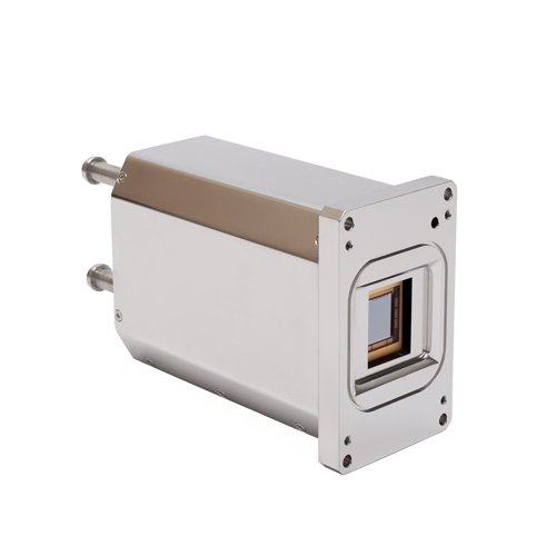
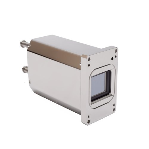
Image sensor: An image sensor is an array of light sensitive pixels in which photons are converted into electric charge. Currently used types are Charged Coupled Devices (CCD) or CMOS based image sensors.
Integration time: The integration time (also exposure time) is the time interval in which the sensor is accumulating electrons in each pixel depending on the incoming light intensity. After the integration time, the image is transferred to a storage region or directly read out.
Interline-transfer CCD image sensor: Next to every pixel is a light insensitive area which is used for the storage of electric charge. After the exposure time the generated electrons in the pixels are shifted into these areas where they are transferred into the readout register. This prevents image smearing during the readout. Since the transfer of charges into the storage registers is fast, pixels can be exposed to light continuously and smearing is prevented. As only part of the pixels is light sensitive, interline transfer cameras have a reduced full-well-capacity and dynamic range compared with full-frame sensors of the same chip size.
Inverted mode operation (IMO): IMO sensors have a modified gate structure which reduces the dark current. In comparison to the standard mode devices, these multi-phase pinned devices have a lower full well capacity. Therefore they have a smaller dynamic range compared to non-inverted mode (NIMO) sensors.
L
M
N
Near-infrared coating: An anti-reflection coating optimized for wavelength ranging from 750 nm to 950 nm.
Non inverted mode operation (NIMO): During charge transfer the input clock signals for the poly-silicon electrodes of one pixel are timed such that the voltage applied to at least one electrode is low. This ensures that the electrons don't mix with electrons from adjacent pixels. Due to defects at the silicon-silicon oxide interface, NIMO sensors have a high dark current which can be reduced by cooling. NIMO sensors have a larger full-well-capacity compared to AIMO sensors.
O
Open electrode: Front-illuminated sensors can have patterned electrodes such that part of the pixels are uncovered from the poly-silicon gate structure and therefore open for direct light exposure. Therefore light absorption by the poly-silicon electrodes is reduced. Image sensors with open electrodes have an enhanced quantum efficiency in the UV range.
Output node: An on-chip circuit into which the charge is shifted from the readout register. The output node converts the collected electrons in each pixel into a voltage and amplifies the signal.
P
Pixel: Pixels are the smallest elements in the light sensitive area of a sensor. They are arranged in rows and columns on an image sensor. The smaller the pixel size, the higher the spatial resolution of the sensor. In larger pixels more electrons can be stored typically, which results in a higher dynamic range.
Pixel readout frequency: The frequency with which the charges in the readout register are transferred pixel by pixel towards the output node.
Poly-silicon electrodes : Gate electrodes are placed on the surface of the image sensor. They control the storage and transfer of charges from pixel to pixel. For charge transport each of the poly-silicon gate electrodes in one pixel receives individual input clock signals. The signals are timed such that the charge is shifted pixel by pixel.
Potential well: A region in the pixels of the CCD sensor where the generated electrons are stored before they are shifted to the readout register. The depth of this region is controlled by altering voltages to the gate electrodes or by special doping of the silicon material.
Q
R
Read noise: In CCD cameras, the read noise is caused in the output node of the sensor which converts the electric charge into a voltage. The read noise increases with higher readout frequency and can not be eliminated. For a high intensity of light and a low readout frequency, the read noise is small compared with the shot noise.
Readout register: The readout register is a row of pixels adjacent to the light sensitive area of the sensor. Charges are transferred from the sensor area into the readout register where they are shifted pixel by pixel to the out-put node on the chip. The readout register is insensitive to light in order to prevent further charge generation during readout.
S
Sensitivity: The sensitivity of scientific cameras is typically given in counts per electron. When photons hit the CCD sensor, there is an accumulation of electrons in the respective pixel. The camera translates the number of stored electrons into a digital representation of the signal.
Shot noise: Due to fluctuation in the emission of every light source, the number of photons that hit the sensor pixels in time may vary. The standard derivation of the statistic distribution of the photon flux is the shot noise.


