


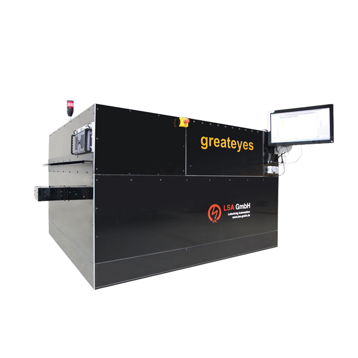

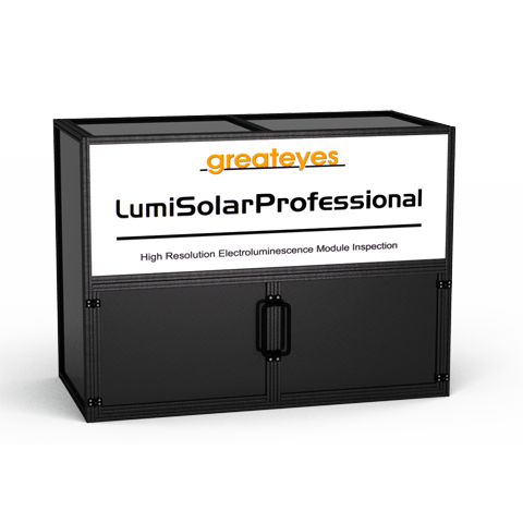
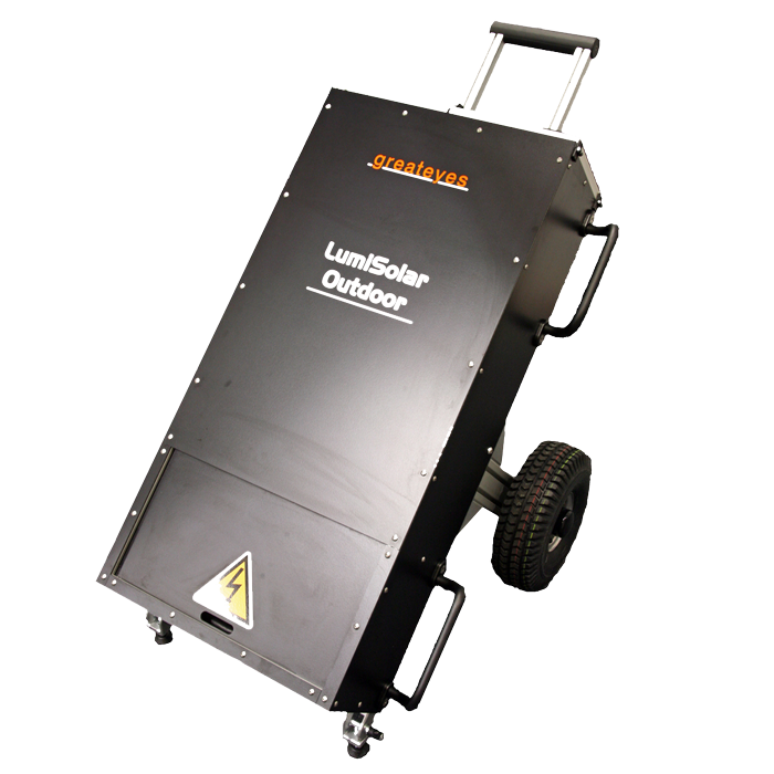

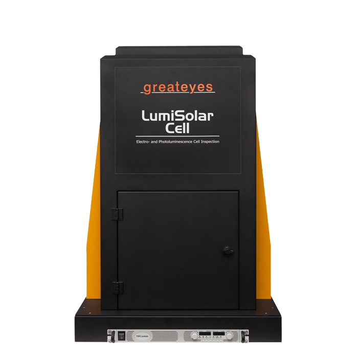


Inspection of Wafer, Solar Cells & Modules
Solar cells and solar modules suffer from a variety of invisible defects which reduce their output power and long-term stability. The highly sensitive Inspection Systems from greateyes image these problems. This allows you to optimize the production, increase output power and reduce overall costs.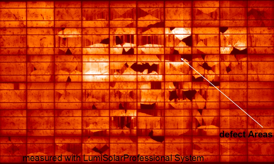 |
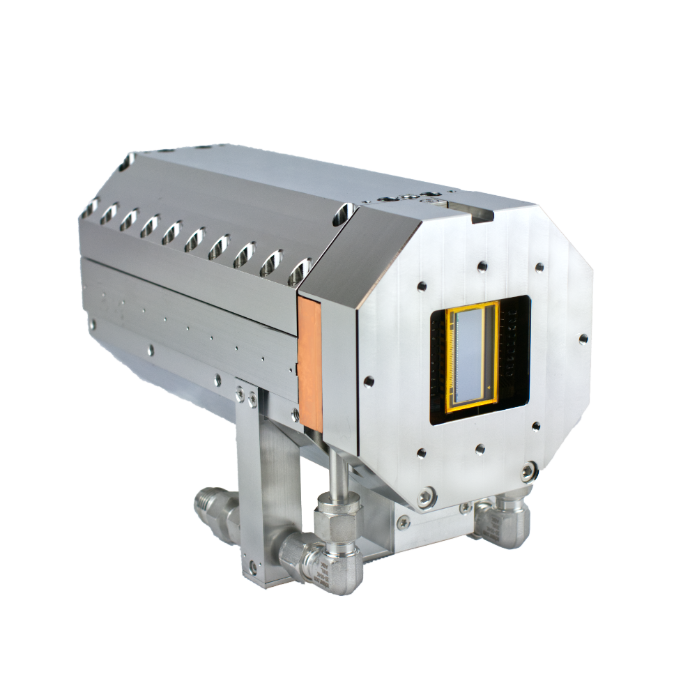
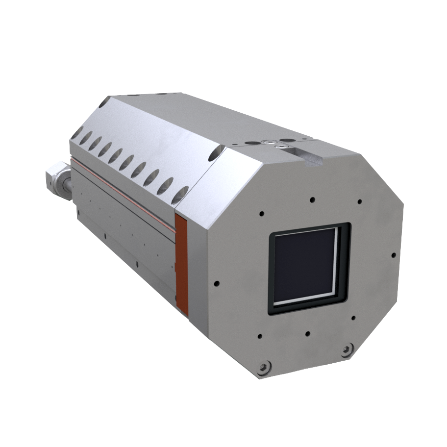
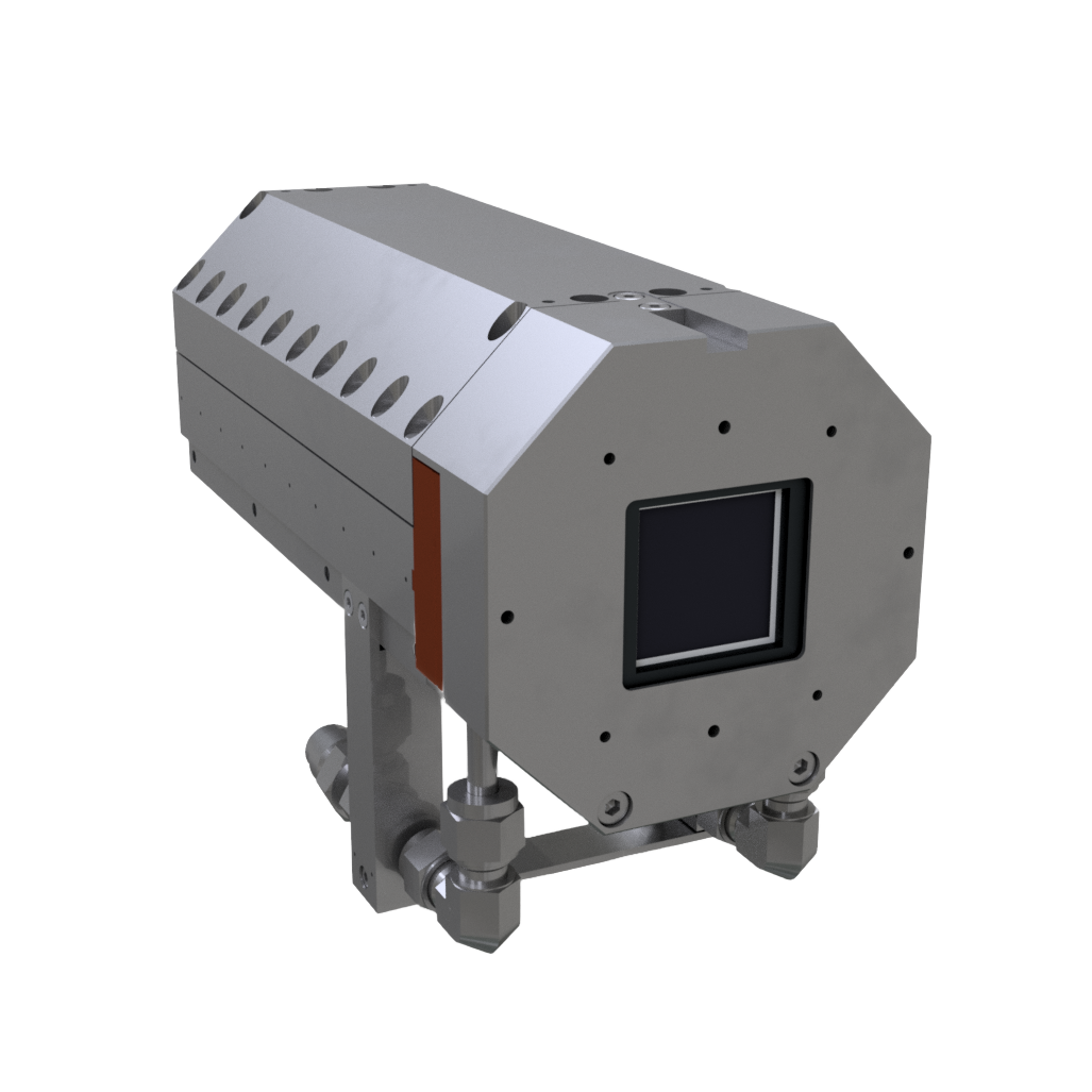
Electroluminescence An external current is applied to the solar cell or module using its electrical contacts. The invisible electroluminscence radiation emitted by the solar cell or module is detected by a highly sensitive camera. |
 |
Photoluminescence The solar cell or wafer is excited by an intensive light source. No electrical connections to the solar cell are necessary. The invisible photoluminescence radiation emitted by the wafer or solar cell is detected by a highly sensitive camera. |
Advantages of Electroluminescence (EL) and Photoluminescence (PL) Inspection
- EL and PL are non-destructive methods
- Measurements deliver detailed information about defects and their location
- EL and PL provide a high informative content, many types of defects can be clearly identified
- Fast measurement on a second timescale
- EL can be used to investigate small cells as well as large areas made from mono-Si, poly-Si, a-Si, micro-Si, CIGS, CIS, CdTe
- Method can be integrated in the production process (in-line)
- EL and PL are also well suited for research and development of new photovoltaic devices
Differences between Electroluminescence (EL) and Photoluminescence (PL) Inspection
| Electroluminescence | Photoluminescence | |
| Requirements | Electrical contacts are necessary. | No electrical contacts needed. |
| Substrates | Solar cells, strings, modules | Wafers, solar cells, as-cut wafers |
| Materials | mono-Si, poly-Si, a-Si, micro-Si, CIGS, CIS, CdTe | mono-Si, poly-Si, a-Si. micro-Si, CIGS |
| Measurement time | 0.2 - 1 sec for mono-Si or poly-Si | 0.2 - 2 sec for mono-Si, poly-Si |
| Informative value | Micro-cracks, shunts, finger defects, deposition problems, bad edge isolation, ... | Micro-cracks, inhomogenities, impurities, dislocations |
Selected References:
S. Roy, S. Kumar, R. Gupta. Investigation and analysis of finger breakages in commercial crystalline silicon photovoltaic modules under standard thermal cycling test. Engineering Failure Analysis, 2019, Volume 101, Pages 309-319
U. Jahn et al. Review on IR and EL Imaging for PV Field Applications.
International Energy Agency, Photovoltaic Power Systems Programme, Report IEA-PVPS T13-10:2018, March 2018
M. Regehly, R. Kemmler. LED-Based Photoluminescence Inspection of Crystalline Silicone As-Cut Wafers.
Poster at the EU PVSEC 2015, Hamburg
C. Peike, S. Hoffmann, M. Heck, T. Kaltenbach, K.-A. Weiß, M. Köhl.
Nondestructive Determination of Climate-Specific Degradation Patterns for Photovoltaic-Module Encapsulation. Energy Technology, 2014, Volume 2, Issue 1, pages 121–129
C. Peike, S. Hoffmann, P. Hülsmann, B. Thaidigsmann, K.A. Weiβ, M. Koehl, P. Bentz. Origin of damp-heat induced cell degradation. Solar Energy Materials and Solar Cells, 2013, Volume 116, Pages 49–54
A. Mansouri, M. Zettl, O. Mayer, M. Lynass, M. Bucher, O. Stern, C. Heller, E. Mueggenburg. Defect detection in photovoltaic modules using electroluminescence imaging. 27th EU PVSEC, 2012
M. Regehly, J. Penlington. Im Einsatz für mehr Strom.
Elektrolumineszenz-Inspektion von Solarzellen und -modulen, Inspect-Online, 3/2012


